
Mastering KiCad PCB Design Rules: A Practical Guide & Template
Many years ago, starting a new PCB design often filled me with anxiety. The sheer number of considerations before even placing a single component felt overwhelming. At the time, I was working at a small company with my dear colleague Jesus. As junior engineers, we intuitively developed a system to alleviate the “starting from scratch” feeling. Without consciously realizing it, we stumbled upon the power of systematization and process.
One of the very first things we defined was a consistent, replicable set of Design Rules (DR). We applied this to every design we worked on and realized that a well-defined and reusable set of DRs significantly minimizes the risk of errors, shortens design time and reduces anxiety 😝.
That’s what this post is about. I’ll show you how I define the Design Rules I systematically apply to all my KiCad designs to ensure they meet both project specifications and manufacturer capabilities. I’ve organized the rules into three areas: manufacturing, project-specific and high-speed signals. Let’s dive in.
Manufacturing Rules
I’ve named “Manufacturing Rules” those directly related to the manufacturing limitations of the PCB supplier I plan to use. These rules include, for example, minimum hole diameter, minimum track width, and minimum clearance. In KiCad those can be found under the “Constraints” section in the tab “Design Rules” of the “Board Setup” dialog (File/Board Setup…).
Remember that stricter requirements often lead to increased production costs, that’s why I systematically chose achievable values as a starting point for all my designs. Fore more complex projects I just change them to the minimum values I need.
The following image shows the values I choose.
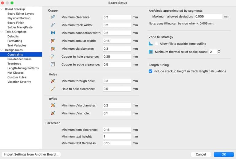
It’s crucial to understand that the minimum values defined in the “Constraints” section are absolute minimums. They cannot be overridden by more specific design rules. For example, in the image above, the minimum clearance is set to 0.2 mm. This means 0.2 mm is the absolute minimum clearance allowed anywhere on the PCB. Even if you define a custom rule or a net class with a clearance setting lower than 0.2 mm, the “Constraint” section’s 0.2 mm value will always take precedence. It’s the absolute floor.
Beyond the “Constraints” section, other manufacturer-related parameters are also critical. Solder mask and paste settings, which are crucial for proper assembly, are configured under the “Board Stackup” tab in the “Solder Mask/Paste” section. Here are my default values for these.
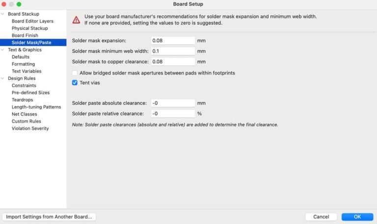
I chose these values based on recommendations of my regular PCB manufacturers and my experience, providing a good balance between ensuring proper solder coverage and preventing solder bridges.
Project-Specific Rules
KiCad offers two primary methods for defining specific design rules. The first, and simplest, involves net classes. You configure these classes and their associated values within the Net Classes section, as illustrated below.
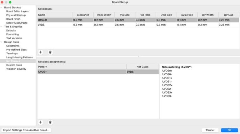
The automatically generated “Default” class reflects the absolute minimum values defined in the Constraints section. All other net classes must adhere to values equal to or exceeding these defaults. For instance, the “HV” (High Voltage) class has a 1 mm clearance, which is the minimum distance copper-to-copper that should be in between a signal belonging to the HV class and any other signal, including those within the HV class itself.
However, this approach has limitations. How, for example can be specified a clearance rule exclusively between HV nets and non-HV nets? This is where the second method, defined Custom Rules, becomes essential.
It is important to remark that all the Custom Rules have always priority over the design rules set on the Net Classes section, except for the “Default” class that is always specifying the global minimum values.
Here are some of the custom rules that I use regularly.
High Voltage
Often, circuits, especially in power electronics designs, contain signals with significantly different voltage potentials. For example, a power electronics stage might handle signals at 100 V, while other sections of the same circuit operate at 3.3 V. In such cases, I create a net class (as described in the previous section) containing all the high-voltage (HV) signals and then define the following custom rule:
# High Voltage clearance 100V
(rule “100V Clearance”
(severity error)
(condition “A.NetClass == ‘HV’ && B.NetClass != ‘HV'”)
(constraint clearance (min 1mm)))
It’s important to note that clearance values should be determined by considering not only voltage levels but also product specifications, safety regulations, materials, and other factors. Unless otherwise specified by the client, for designs connected to mains power or involving high voltages, I consult IEC 60664-1 for appropriate clearance values. For designs with less stringent requirements and lower voltages, I typically use IPC-2221.
Thermal Relief Connections
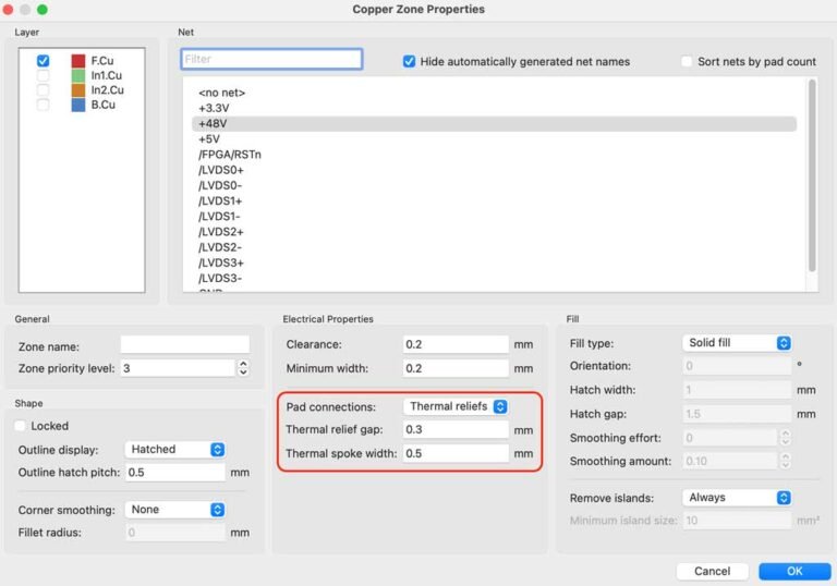
Working with Filled/Copper Zones in KiCad (Polygon Pours for those familiar with Altium Designer 😉) requires special attention to how the zones connect with component pads. Thermal relief connections are generally the preferred method for improving solderability. However, determining the appropriate thermal relief gap and spoke width can be challenging when dealing with a variety of component sizes. Here’s my approach.
I begin by setting the thermal relief gap and spoke width in the properties menu of the Filled Zone. This initially applies the same connection settings to all components. The following image shows an example configuration:
Here’s how the connections look with these global settings:
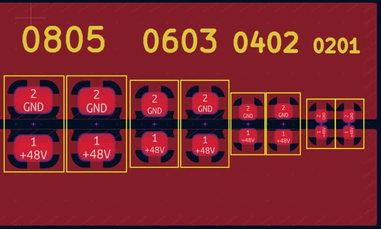
As you can see in the image above, with a thermal relief gap of 0.3 mm and a spoke width of 0.5 mm, the connections for smaller components, such as 0402 and 0201 packages, are far from ideal. KiCad automatically has adapted the resultant connections of those pads, but we don’t have control over it.
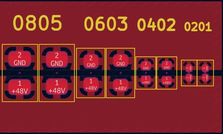
To address this, I’ve created a custom rule that sets the thermal relief gap and spoke width to 0.2 mm and 0.25 mm, respectively, for these smaller components.
# Filled Zone thermal relief connection on sizes from 0402 and 0201
(rule “Thermal relief on 0402 and 0201”
(severity error)
(condition “A.memberOfFootprint(‘Capacitor_SMD:C_0402_1005Metric’) || A.memberOfFootprint(‘Resistor_SMD:R_0402_1005Metric’) || A.memberOfFootprint(‘Capacitor_SMD:C_0201_0603Metric’) || A.memberOfFootprint(‘Resistor_SMD:R_0201_0603Metric’)”)
(constraint thermal_spoke_width (min 0.25mm))
(constraint thermal_relief_gap (min 0.2mm)))
The following image demonstrates the improved thermal relief connections for components with 0402 and 0201 packages:
For those interested in learning more about selecting appropriate thermal relief gap and spoke width values, I recommend consulting IPC-2222.
Here is another common scenario where a custom rule is necessary to manage copper zone connections. As mentioned earlier, thermal relief connections are generally preferred for assembly reasons. However, this isn’t always the optimal approach, especially for components that dissipate significant power, such as the LDO shown below.
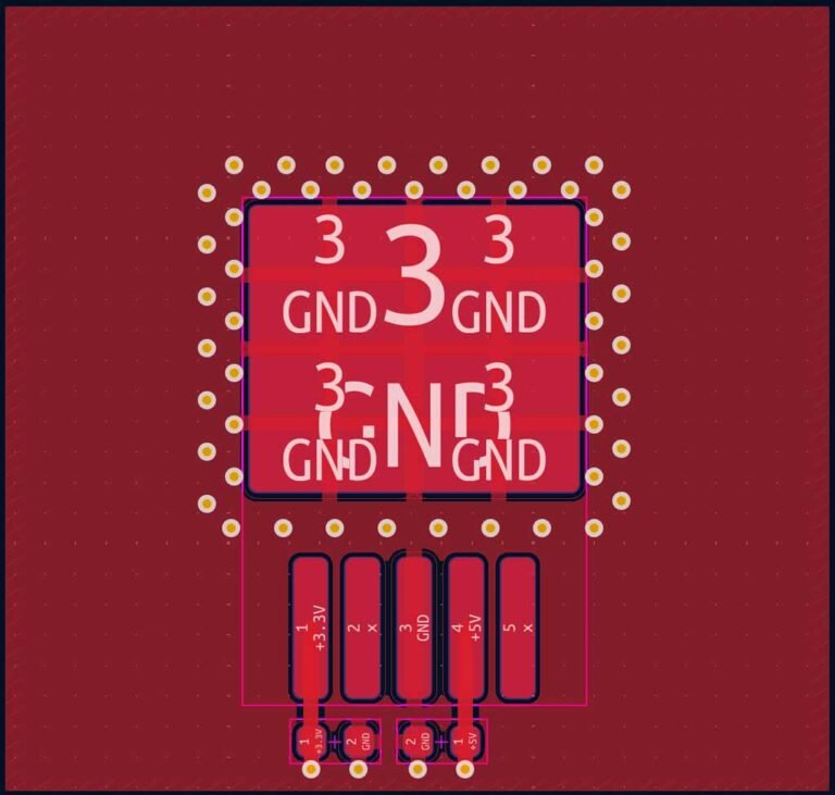
Notice that the GND plane, intended to dissipate heat from the LDO, is connected to the thermal pad via thermal reliefs. While changing the connection style in the filled zone’s properties to “Direct Connection” solves the LDO issue, it creates a new problem: the input and output capacitors will also be directly connected, which is usually undesirable for the reasons conveyed earlier.
My solution is to keep the copper zone’s “Pad Connections” option set to “Thermal Relief” by default, as most components don’t require direct connections. For those that do, I utilize the following custom rule:
# Filled Zone direct connections
(rule “Direct connections”
(severity error)
(condition “A.memberOfFootprint(‘Package_TO_SOT_SMD:TO-263-5_TabPin3’)”)
(constraint zone_connection solid))
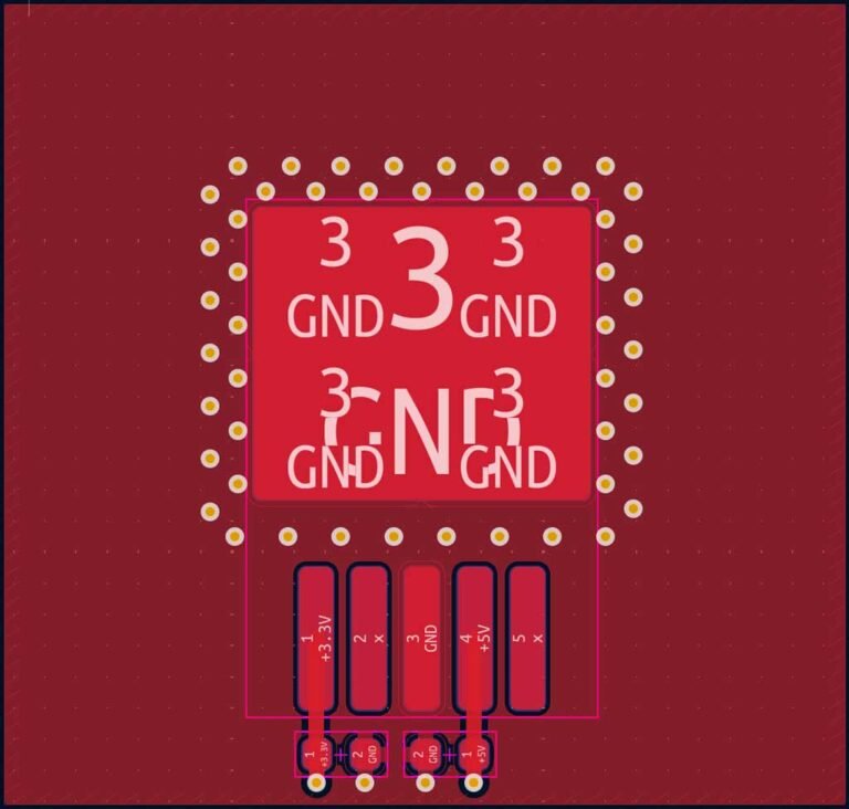
The image below demonstrates the result after applying the custom rule. The copper zone now has a direct connection to the LDO footprint while maintaining thermal relief connections for the capacitors.
Finally, KiCad offers another way to control copper zone connections: by adjusting the pad properties of individual components. This could be applied, for example, to the pad number 3 of the LDO.
However, this technique requires manual configuration for each pad and component, making it a tedious and impractical approach for most situations. Consequently, I rarely use this option.
High-Speed Signals Rules
The design rules presented here could easily fit in the previous section, but I decided to dedicate a separate one to them. This is a critical topic that deserves special attention, and it’s not something I include in all my designs.
When I have impedance-controlled signals in my design, I always define a net class for each target impedance. In the example below, there are LVDS signals (100 Ohm differential) and a 50 Ohm single-ended signal. The net classes are shown in the following image.
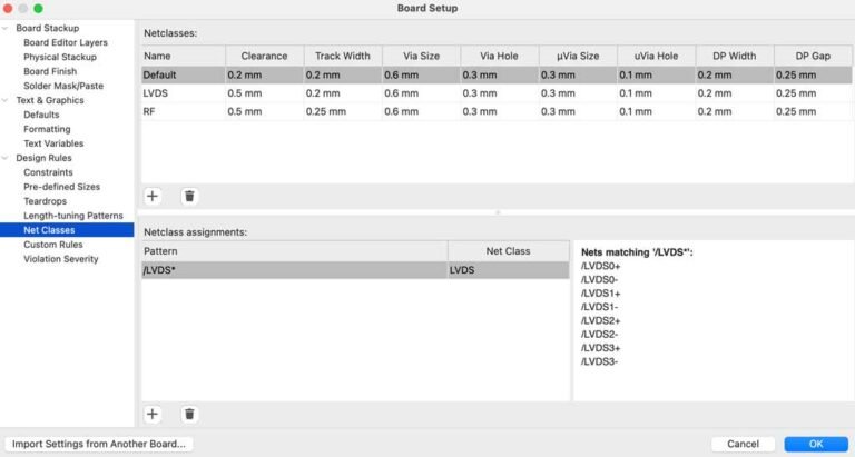
Note that the track width has been set for both the single-ended and differential signals, as well as the gap for the differential pair.
This approach is often sufficient, but I prefer defining custom rules for greater flexibility. Custom rules allow me to set impedance matching parameters based on the layer and also define minimum, optimal, and maximum values. Here are the custom rules I typically use for my high-speed designs.
Single-ended Signals
(rule “Single-Ended Outer 50Ohm”
(severity error)
(layer outer)
(condition “A.NetClass == ‘RF'”)
(constraint track_width (min 0.24mm) (opt 0.25mm) (max 0.26mm)))
(rule “Single-Ended Inner 50Ohm”
(severity error)
(layer inner)
(condition “A.NetClass == ‘RF'”)
(constraint track_width (min 0.23mm) (opt 0.24mm) (max 0.25mm)))
Differential Pair Signals
(rule “Differential Outer 100Ohm”
(severity error)
(layer outer)
(condition “A.NetClass == ‘LVDS'”)
(constraint diff_pair_gap (min 0.2mm) (opt 0.2mm) (max 0.21mm))
(constraint track_width (min 0.2mm) (opt 0.2mm) (max 0.21mm)))
(rule “Differential Inner 100Ohm”
(severity error)
(layer inner)
(condition “A.NetClass == ‘LVDS'”)
(constraint diff_pair_gap (min 0.17mm) (opt 0.18mm) (max 0.19mm))
(constraint track_width (min 0.17mm) (opt 0.18mm) (max 0.19mm)))
Conclusion
This post has shown only a few examples of the design rules I frequently use in my KiCad designs. Naturally, every project has its own unique requirements and characteristics, but the rules presented here can serve as a foundation for consistent and reliable designs, reducing the likelihood of errors.
To achieve the systematization mentioned earlier, instead of configuring all these rules for each new design, I start with my KiCad base project, available in my GitHub repository. This template incorporates all the design rules discussed in this post, providing a solid foundation for your own PCB designs. I encourage you to use it: it will significantly streamline your workflow and reduce the risk of errors.
If you think I’ve missed something important, please let me know in the comments. I’ll consider including it on GitHub or perhaps addressing it in a follow-up post.
Adw!